 |
Bookmark | Contact Us |
 Technical support

-
- Technical support
01��NO signal output from the crystal ?
1-1.
Please measure the signal output by two terminals of the crystal using Oscilloscope or Frequency Counter. If there is no signal output, please follow step 1-1 to step 1-4 to execute the examination. If there is signal output from out- terminal of the crystal ( Xout), but no signal output from the in-terminal (Xin), please check the crystal following step1-5 to step 1-6.
1-2.
Please uninstall the crystal and test its frequency and load capacitance to see whether they vibrate and meet your specifications using a professional testing machine. You can also send it to your supplier to have them test it for you.
1-3.
If any of the following situations happen, the crystal doesn��t vibrate, its load capacitance doesn��t match your specification,
or there is a huge gap between current frequency and your targeted frequency, please send the crystal to your supplier to conduct Quality Analysis. If the frequency and load capacitance meet your specifications, we will need to conduct
Equivalent Circuit Test.
1-4.
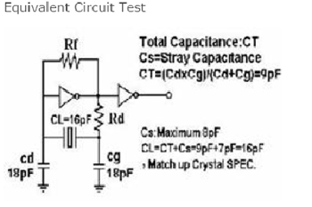
Equivalent Circuit Test

1-4-1.
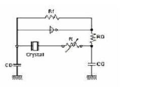
Generally, the oscillation circuit of Microprocessor derives from Colpitts circuit showing below:
Picture 1
Cd and Cg are external load capacitances, which have been built in the chip set. (Please refer to the Specifications of the
chip set)
Rf is the feedback resistance with200K��~1M��. It��s built in the chip set generally.
Rd is the Limit Resistor with 470��~1K��. This resistance is not necessary for common circuit but only for circuits having
high power supply.
1-4-2.
A stable oscillation circuit requires a negative resistance and its value should be at least five times of the crystal
resistance. It can be written as |-R| > 5 Rr.
For example, to acquire a stable oscillation circuit, the value of negative resistance of the IC must be under �C200�� when
the value of the crystal resistance is 40��.
1-4-3.
��Negative resistance�� is the yardstick to evaluate the quality of an oscillation circuit. Under some circumstances such as
aging, thermal change, voltage change, and etc., the circuit might not oscillate if the value of �� Q�� is low. Thus, it��s very
important to measure the negative resistance (-R )following the instructions below:

(1) Connect the resistance (R) with the crystal in series
(2) Adjust the value of R from the start point to the stop point of the oscillation.
(3) Measure the value of R during oscillating.
(4) You will be able to obtain the value of negative resistance, |�CR| = R + Rr, and Rr = crystal resistance.
P.S. the stray capacitance of the connected circuit might affect measured values.
1-4-4.
If the parameters of the crystal are normal but it��s not working steadily within the oscillation circuit, we will have to find
out whether the resistance value of the IC is too low to drive the circuit. If that��s the case, we have three methods to
improve such situation:
Lower the value of external capacitance(Cd and Cg), and adopt other crystal with lower load capacitance (CL).
Adopt a crystal with lower resistance (Rr).
Use the design of unequal values of Cd and Cg. We can increase the load capacitance of Cd (Xout) and decrease the
load capacitance of Cg(Xin) to raise the output of waveform amplitude from Xin which will be used in its back-end
circuit.
1-5.
When there is signal output from Xout but not Xin, it represents the case that the power consumption of the rear -
electrode Backend Circuit is extremely huge. We can add a buffer between the output of the circuit and its rear electrode
to drive the back-end Circuit.
��
1-6.
Except the method of 1-5 mentioned above, you can also follow the three methods in step 1-4-4. Please
contact the field application engineers of crystal or IC manufacturers for further assistance, if your problem can��t be
solved.
02. System is not functioning because of no adequate output waveform amplitude from the crystal ?
2-1.
Please measure the signals from the two terminals of the crystal using Oscilloscope or Frequency Counter, if the Frequency
is not within the specification and it��s output waveform amplitude is not adequate (for example, over+/- 200ppm), please
follow step 2-3 to step 2-5.
2-2.
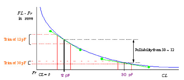
The formula for Capacitances versus Frequency is as following:
�� FL = FR * ( 1 + C1 / 2 * ( C0 + CL) ) where

The curve represents the variation of capacitance changes versus variation of frequency changes ( Frequency pullability):

If the frequency measured by Frequency Counter is higher than the targeted frequency, we should increase the value of
capacitances (CL, or Cd & Cg ) to lower the frequency to the targeted frequency, vice versa.
Please check whether the waveform amplitude is improved or not after we adjust the frequency. If it��s improved, that
indicates the case that the original design of the circuit is not tuned to the best resonant point for the crystal. The crystal
should function normally after the resonant point is adjusted.
2-3.
If the waveform amplitude is not improved even the frequency is pretty much close to the targeted frequency, we can
improve it using three methods below:
Method 1: Lower the value of external capacitance (Cd, and Cg) , and adopt crystal with lower load
������������apacitance (CL).
Method 2: Adopt the crystal with lower resistance(Rr).
Method 3: Use the design of unequal values of Cd and Cg.
We can increase the load capacitance of Cd (Xout) and decrease the load capacitance of Cg(Xin) to raise the output of
waveform amplitude from Xin which will be used in its back-end Circuit.
We suggest that you use above methods to save costs and assure safety
2-4.
Please use the Frequency Counter to measuring the crystal to ensure that the adjusted frequency still meets original
specification after the waveform amplitude has been improved. If the frequency doesn��t meet the specification, please
adopt a crystal with suitable CL value according to your targeted frequency.
2-5.
Please adopt a crystal with lower CL if the frequency is much higher than the targeted frequency, vice versa.
03. System is not functioning due to high deviation of output frequency ?
3-1.
We can improve the problem that deviation of frequency output is over the limit by following methods:
Adjust the values of external capacitance, Cd & Cg.
If the frequency measured by Frequency Counter is higher than targeted frequency, we should increase the external
capacitance, CL ( or the values of Cd & Cg ), to lower the frequency to our targeted frequency, vice versa.
Adopt a crystal with different value of capacitance(CL).
Adopt a crystal with lower capacitance if the frequency is much higher than the targeted frequency, vice versa.
3-2.
Please check whether the waveform amplitude is normal or not using Oscilloscope, after the correct capacitance is adopted
and the frequency is adjusted to target. Under the situation that the waveform amplitude is shrunk due to adding external
capacitances, please use method 2 to adjust the frequency ( lower external capacitances and adopt a crystal with lower
capacitance).
Copyright: Beijing Candor Electronics Co., Ltd.
Add:No.16, Yumin Street, Area B, Tianzhu Airport Industrial Zone,Beijing, P.R.China Postcode: 101318 Fax: +86-10-80483125
Tel: +86-10-80483105 (Ext.104, 105,107,113,118) E-mail: sale@mail.candor-co.com
